Here is a brief presentation of one of my favourite projects. This is not meant to be a complete and technical presentation, but the global scopes of the project.
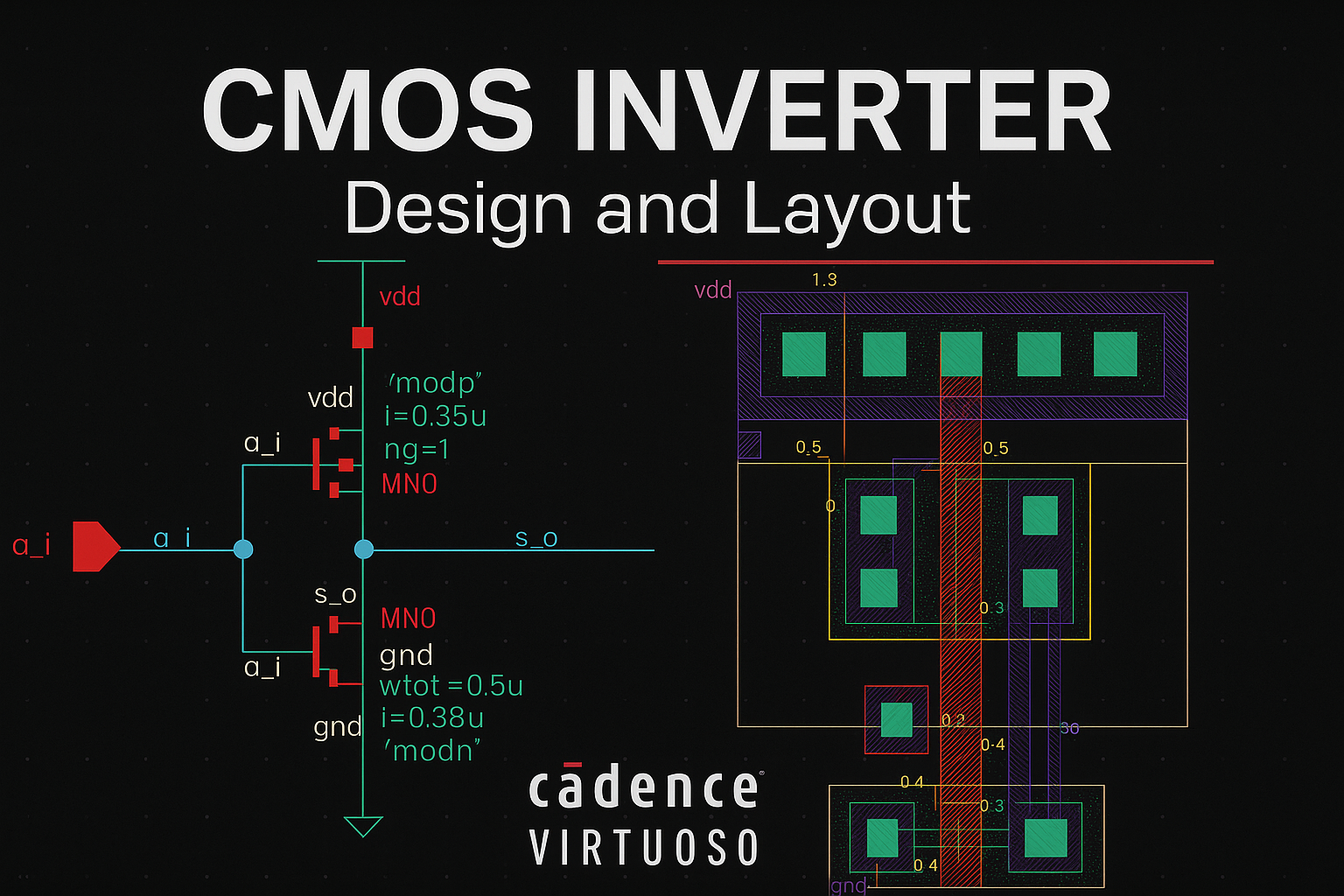
The goal of this project was to design, simulate, and implement the physical layout of a CMOS inverter using Cadence Virtuoso. The project was carried out on the AMS 0.35 µm (C35B4) technology node, providing hands-on experience with an industry-grade process design kit (PDK).
Project Workflow
Schematic Design
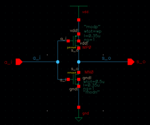
Built the inverter at the transistor level with NMOS and PMOS devices.
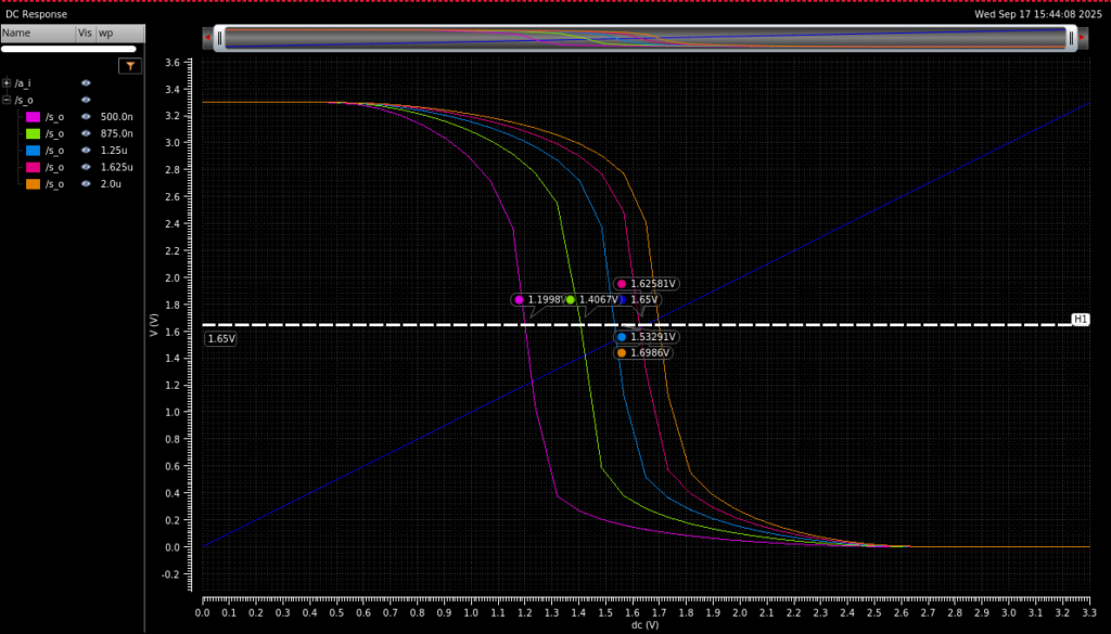
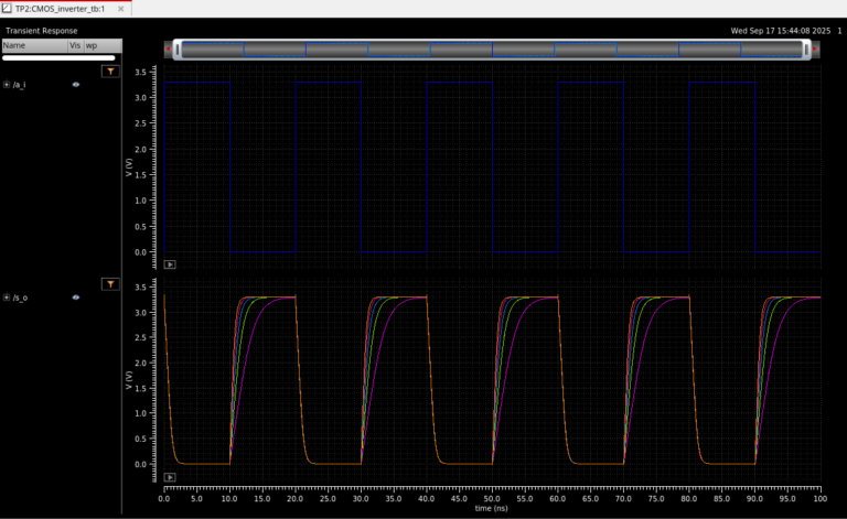
Performed DC simulations to extract the Voltage Transfer Characteristic (VTC).
Ran parameter sweep on MOS Width to optimize the inversion.
Layout Implementation
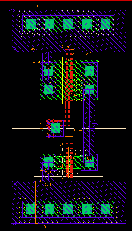
Designed the full custom layout of the CMOS inverter following AMS 0.35 µm design rules.
Adjusted transistor sizing to balance performance and technology requirments.
Verification
Performed Design Rule Check (DRC) to ensure compliance with AMS design rules.
Conducted Layout Versus Schematic (LVS) to confirm consistency between schematic and layout.
Extracted parasitics (PEX) and ran post-layout simulations to evaluate performance degradation caused by layout effects.
Used Tools
Cadence Virtuoso for schematic, simulation (ADE XL) , and layout (Layout XL)
AMS 0.35 µm (C35B4) CMOS technology
SPICE simulations for electrical validation (DRC, and LVS)
Layout
Layers MET1, POLY1, NDIFF, NPLUS
Used DRM to ensure size and design constraints respect