Here is a brief presentation of one of my favourite projects. This is not meant to be a complete and technical presentation, but the global scopes of the project.
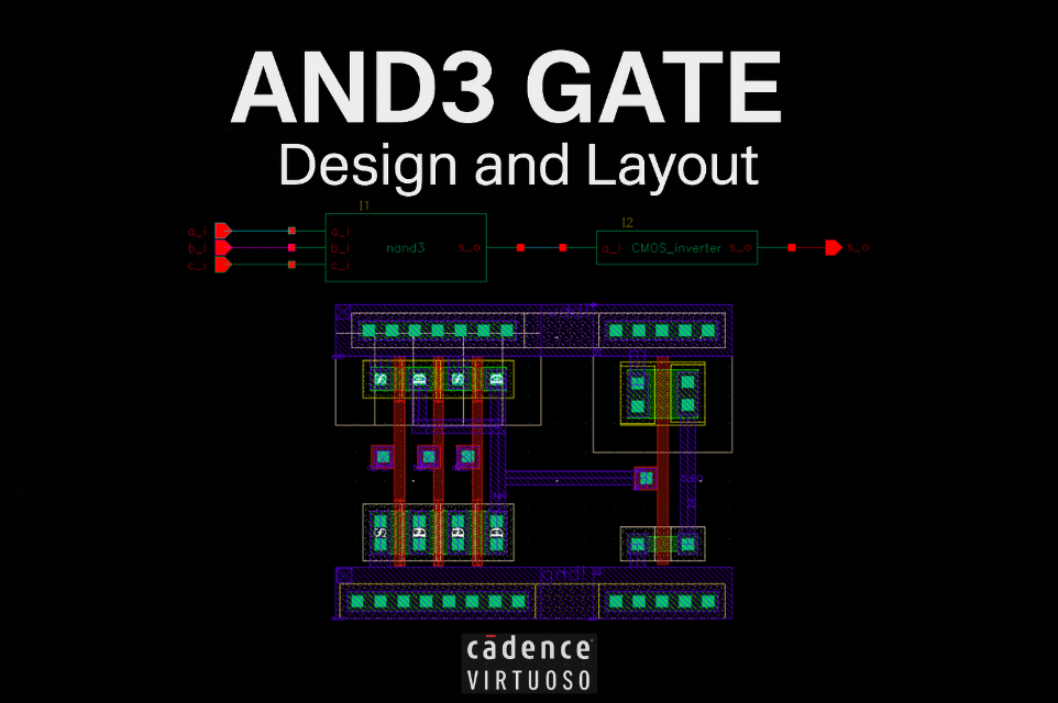
This project focuses on the design and layout of a 3-input CMOS AND gate (AND3) using Cadence Virtuoso and the AMS 0.35 µm technology. The goal was to complete a full custom design flow — from schematic to post-layout simulation — and to analyze the impact of parasitics on timing performance.
Project Workflow
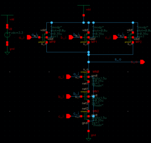
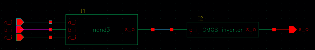
Schematic Design
Created the logic structure using a NAND3 + Inverter implementation for efficiency. (See CMOS Inverter project)
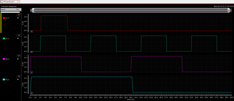
Pre-Layout Simulation
Performed Simulations to ensure the logical functionality
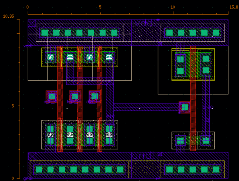
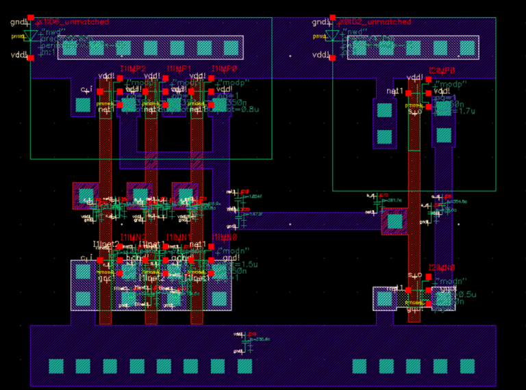
Layout design
Built the physical layout of the NAND3 Gate in Virtuoso Layout‑XL using Euler paths to minimize diffusion breaks and area.
Reused the existing CMOS Inverter layout from the previous project
Verification
Performed Design Rule Check (DRC) to ensure compliance with design rules.
Conducted Layout Versus Schematic (LVS) to confirm consistency between schematic and layout.
Extracted parasitics (PEX) and ran post-layout simulations to evaluate performance degradation caused by layout effects.
Used Tools
Cadence Virtuoso for schematic, simulation (ADE XL) , and layout (Layout XL)
AMS 0.35 µm PDK (C35B4) CMOS technology
SPICE simulations for electrical validation (DRC, and LVS)
Layout
Used the “Generate from Cellview” feature to automatically produce a layout template and speed up the process for the NAND3 Layout.
Reused the existing inverter layout from a previous project to ensure consistency and save time.
Used DRM to ensure size and design constraints respect
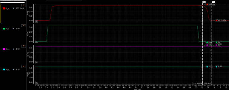
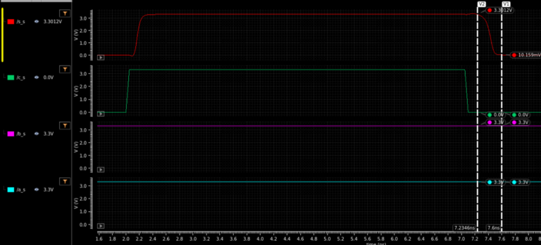
Parasitic Extraction
Generated an extracted view including parasitics.
Impact on performance
There is a performance degradation due to parasitic capacitances
We can see that the propagation delays are higher after Layout